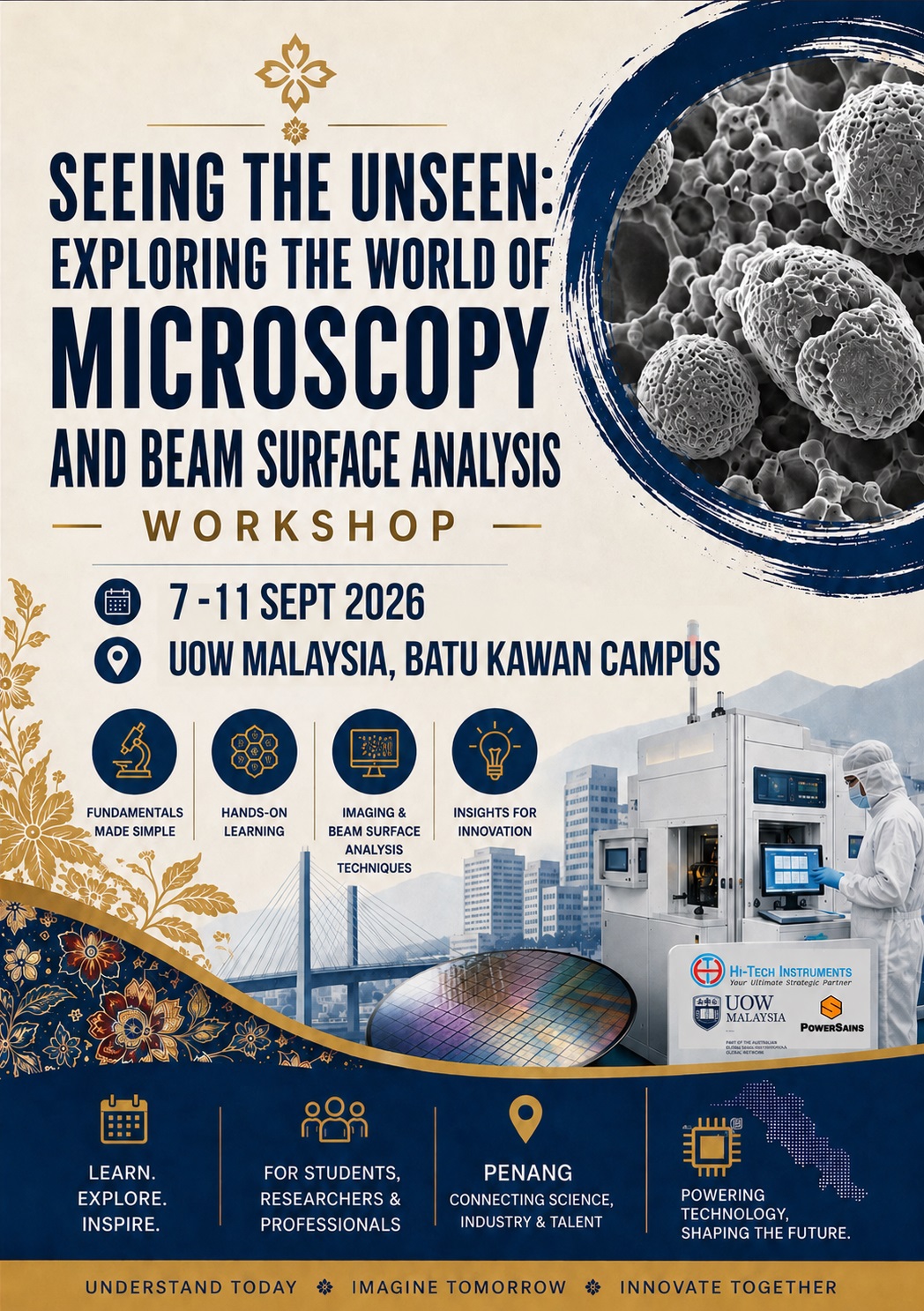
Welcome to the Seeing the Unseen: Exploring the World of Microscopy and Beam Surface Analysis Workshop 2026 event page!
Mark your calendar for the 7 - 11th September 2026 - Seeing the Unseen: Exploring the World of Microscopy and Beam Surface Analysis Workshop 2026 is going to rock Penang.
Seeing the Unseen:
Exploring the World of Electron Microscopy and Surface Beam Analysis.
University of Wollongong, Batu Kawan Campus, Batu Kawan, Penang.
7th – 11th Sept, 2026
This workshop is designed to equip your engineers and technicians with the fundamentals of electron microscopy and particle beam methods for advanced material analysis and sample preparation. Stay ahead of industry standards, sharpen your team's technical edge, and discover how these cutting-edge methods can directly solve your company’s quality control challenges.
In this workshop, participants will explore the inner workings of electron microscopes and the various techniques that maximize data collection for problem solving. You will get to know the latest instrumentations and frontier technologies in this area. Additionally, you are invited to bring your own samples for on-site analysis using the Hitachi SU3800 IPT VP-SEM. Take this unique opportunity to have your materials evaluated by experts with decades of experience from Hi-Tech Instruments, receive tailored advice, and engage in meaningful discussions with other professionals practicing in the field.
Seeing the Unseen: Exploring the World of Microscopy and Beam Surface Analysis Workshop 2026 registration is now open!
Objectives:
* Latest science and guidelines
* Expert-led talks and hands-on sessions
* Regional and international perspectives
* Networking with leaders in electron microscopy and technology
Hitachi SU3800 VP-SEM for High-Performance Microanalysis
The SU3800 in action:
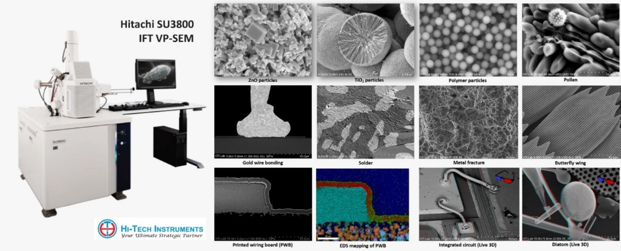
Features:
-
Zero-Preparation Imaging: Variable pressure mode enables quick observation of non-conductive and biological specimens.
-
Intelligent Automation: Features Intelligent Filament Technology (IFT) for 3x longer filament life and auto-adjustments for rapid data acquisition.
-
Seamless Navigation: Integrated camera system (SEM MAP) allows smooth tracking across the entire sample area.
Participation Details
RM200 : Covering Talks, Demonstration of the Hitachi SU3800 IPT VP-SEM,
Campus Tour and Lunch on 7th and 8th Sept
RM300 per session :
For 1 session of sample analysis ( 2 – 3 hours) using the Hitachi SU3800 IPT VP-SEM
There shall be 5 sessions. You can book more than 1 session.
For sessions time – see attached schedule.
In conjunction with this workshop, we have planned to bring school and university students to expose them to the world of micro-analysis as part of the of the STEM promotion initiative among schools. We would be grateful if your company can sponsor to cover the expenses related to the cost bringing the students on campus to experience the working of technology .
All sponsors will have their company or names on public materials disseminated related to the Workshop- flyers, programs, banners and relevant projected visuals.
|
Amount of sponsorship |
Free Attendance |
Free Sample Analysis |
|
RM1000 |
1 pax |
1 session ( 1 hours) |
|
RM3000 |
3 pax |
2 sessions (2 hours) |
|
RM5000 |
5 pax |
3 sessions ( 3 hours) |
For more information and registration, please do visit the Howei platform HERE, Facebook page HERE or email us at helpdesk@howei.com
Registration Fees
Electron Microscopy Workshop Registration Fees
The following fees are for the Electron Microscopy Workshop held at Univ of Wollongong, Batu Kawan, Penang on the 7th to 11th of Sept.
Please note all information collected in this form is for the purpose of facilitating the organizing of this event and will not be used for any other purposes or shared with parties outside the organizing committee.
Attendance Fees: RM200
The fee for this event covers the cost for all sessions on 7 and 8th Sept of the event and includes two lunches and morning and afternoon tea.
Electron Microscopy Sample Analysis Fees
RM200 per session (1 hour)
We are looking for sponsors for school students to participate in this event to expose them to the high-tech world of micro analysis. If your company sponsors this event, up to 5 of your company's staff can participate for free, depending on the level of sponsorship.
| Amount of Sponsorship | Free Attendance | Sample Analysis Session |
|---|---|---|
| RM1000 | 1 pax | 1 Session (1 hour) |
| RM3000 | 3 pax | 2 sessions (2 hours) |
| RM5000 | 5 pax | 3 sessions (3 hours) |
This training is conducted by HRDF Accredited trainers, so it is HRDF claimable.
Program & Speakers
|
 |
||
|
Biography Dr. Khong holds a PhD in Solid State Physics. His distinguished career spans executive leadership roles across semiconductor manufacturing, data storage technology, microprocessor assembly, and the solar energy sector, alongside extensive contributions to academia as a university professor and faculty dean. A veteran organizer, he was instrumental in the greenfield startup of two manufacturing facilities and two private universities. Prior to founding PowerSains, he served as the CEO of Tech Dome Penang, playing a pivotal role in the inception, launch, and strategic growth of the world-class science center. In recognition of his foundational contributions to STEM promotion, he was conferred the Darjah Johan Negeri (DJN) by the Penang State Government in 2018. |
||
|
Dr. Yeoh Lai Seng Catching the Invisible: The Microchip Detective's Guide to Failure Analysis |
|
Biography Dr. Yeoh Lai Seng is currently a Lead Principal Engineer in the Failure Analysis Department at Infineon Technologies Memory Solutions Malaysia Sdn. Bhd., where he has been serving since 2010. As a technical lead, he manages a team of engineers supporting the memory product division, with expertise spanning Flash Memory, FRAM, RRAM, SRAM, HyperRAM, eCT memory, and SONOS memory.
Dr. Yeoh Lai Seng is currently a Lead Principal Engineer in the Failure Analysis Department at Infineon Technologies Memory Solutions Malaysia Sdn. Bhd., where he has been serving since 2010. As a technical lead, he manages a team of engineers supporting the memory product division, with expertise spanning Flash Memory, FRAM, RRAM, SRAM, HyperRAM, eCT memory, and SONOS memory.
He holds a Bachelor in Applied Physics from USM (2001), first Master in Solid State Physics from USM (2004), second Master in Microelectronics Engineering from MMU (2011), and a Ph.D. in Semiconductor (GaN-based MOSFET) from USM (2014).
He holds a Bachelor in Applied Physics from USM (2001), first Master in Solid State Physics from USM (2004), second Master in Microelectronics Engineering from MMU (2011), and a Ph.D. in Semiconductor (GaN-based MOSFET) from USM (2014). |
||
| Title Catching the Invisible: The Microchip Detective's Guide to Failure Analysis |
||
|
Abstract
This presentation explores the critical field of semiconductor failure analysis (FA) and its evolution into a strategic driver of "yield maturity" in modern memory manufacturing. As memory devices shrink to nanometer dimensions, physical defects—such as micro cracks, corrosion, and metallic contaminants— become increasingly invisible to conventional inspection methods, threatening both production yield and long term reliability. Drawing on real industrial case studies from Flash memory, flip flop circuits, and advanced packaging, this session introduces cutting edge diagnostic techniques including nano probing, Electron Beam Absorbed/Induced Current (EBAC/EBIC), high resolution STEM imaging, and advanced Energy Dispersive X ray (EDX) spectroscopy. Attendees will learn how these powerful tools not only shorten analysis turnaround time from days to hours, but also uncover root causes—such as tungsten particles from CMP residues and cobalt stringers from silicidation processes—that lead to measurable yield improvements of up to 4% and >60% reduction in defect rates for automotive applications. The webinar also addresses the emerging challenges posed by 3D packaging technologies like Through Silicon Vias (TSVs) and hybrid bonding, and looks ahead at future enablers such as Plasma FIB and machine learning assisted defect classification. This session bridges fundamental semiconductor physics with industrial manufacturing reality, demonstrating why failure analysis is the unsung hero behind every reliable smartphone, computer, and automotive electronic system. |
|
Dr. Azdiar A. Gazder Multiscale Analytical Microscopy |
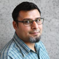
|
Biography
|
||